
Organic electronics is an emerging technology that promises to cover a wide range of applications exploiting the intrinsic characteristics of the organic materials: low temperature process, flexibility, biocompatibility and even the biodegradability. Among the most recent applications, it can be mention: organic electronic circuits driving electrophoretic ink display, electronic skin that use devices on ultrathin substrates and on stretchable substrates, implantable devices that exploit the biocompatibility of organic materials. Furthermore, sensor applications take advantage from the wide range of different organic materials available for electronic devices and from the different device structures allowed by organic technology. The simple structure of organic electrochemical transistors (OECT) allows their use for chemical and biological sensing applications: control cell activity, simple wearable sensors, new devices for bioelectronics. Basic devices for organic electronics are thin film transistors (OTFTs), whose performance is continuously improving in the last years thanks to the development of new organic materials, specifically designed to obtain high carrier mobility and high stability.
The group on organic electronics in IMM-Rome developed fabrication process for organic thin film transistors (OTFTs) with evaporated and solution processed organic semiconductor.
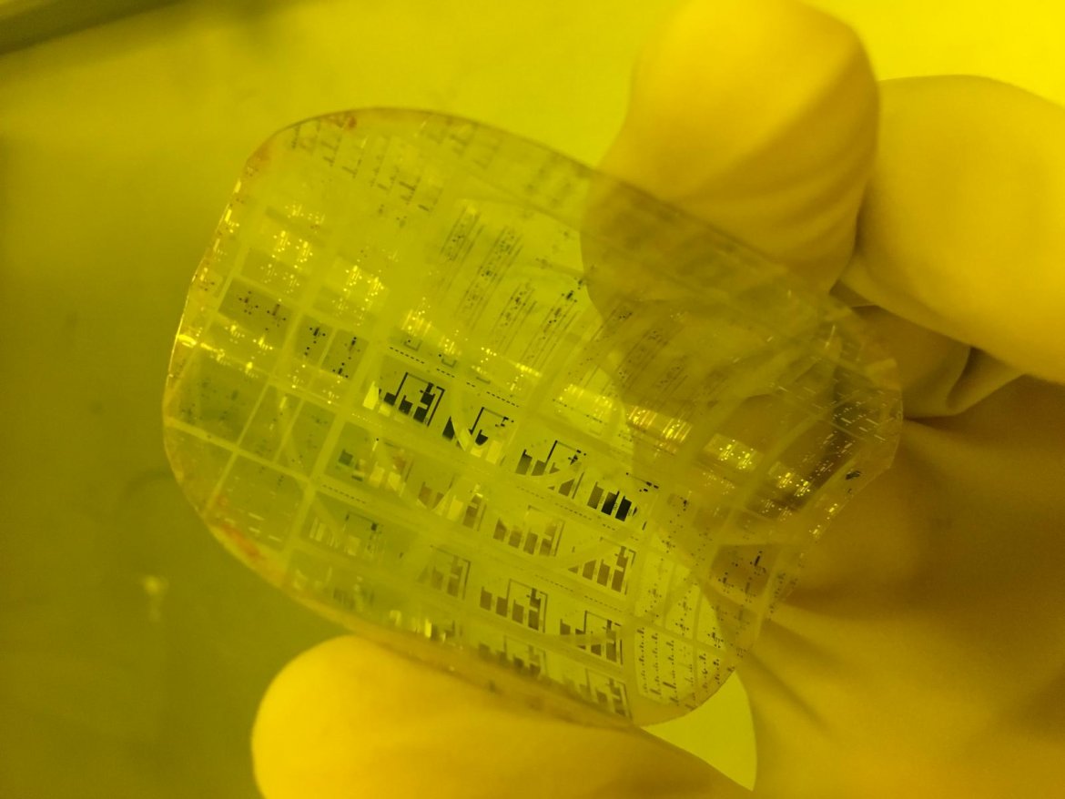
Devices with evaporated organic semiconductors
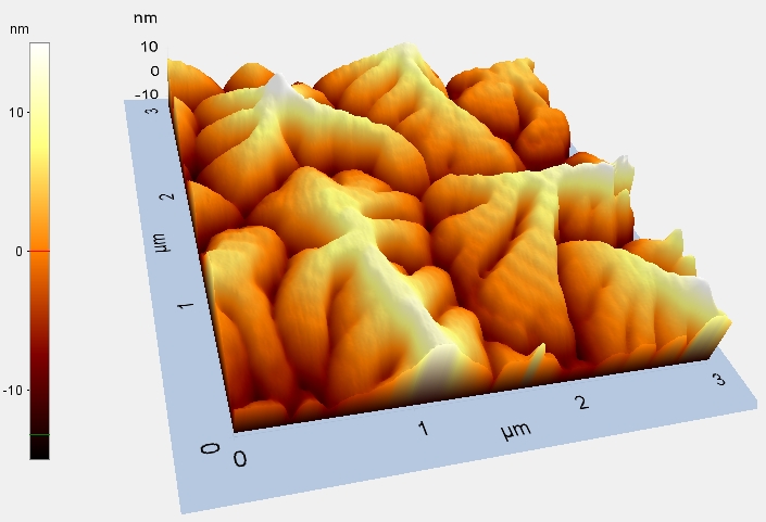
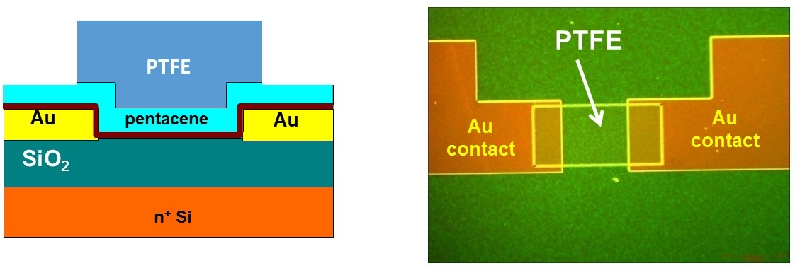
OTFTs with pentacene and DNTT evaporated semiconductors have been fabricated and their electrical characteristics have been studied with particular attention to the long-term device reliability. Several passivation layers have been investigated in order to reduce the environmental effects on the devices.
Devices and circuits with solution processed organic materials
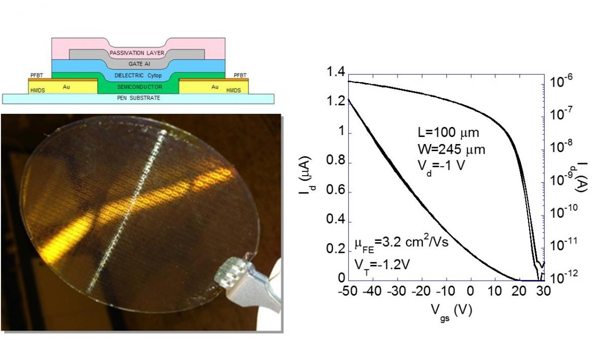
High performance OTFTs have been fabricated with with solution processed organic semiconductors and gate dielectric, deposited by spin-coating technique, and standard photolithigrafic processes. The maximum process temperature is 100 °C allowing the used of flexible plastic substrates (polyethylene naphthalate, PEN). The organic devices shows excellent electrical characteristics (high mobility, low threshold voltage, high electrical stability) allowing their used in organic circuits, as inverters and ring oscillators.
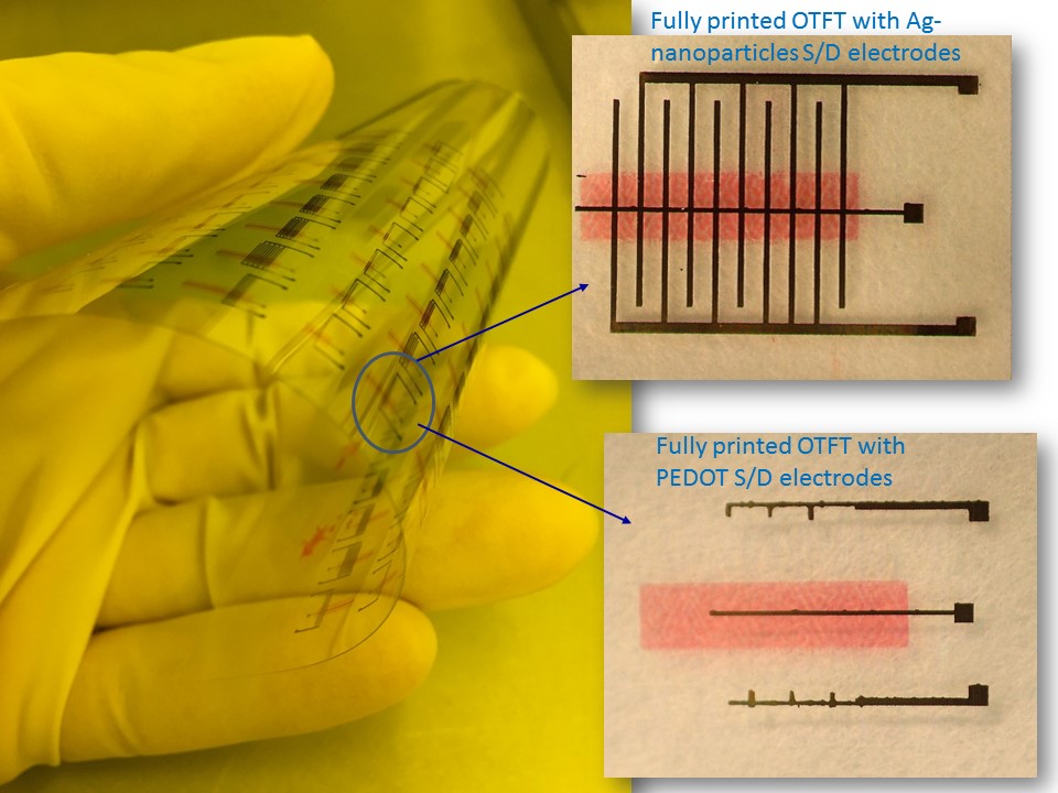
Fully printed OTFTs
Fully printed organic thin film transistors have been developed by using different printing techniques. In particular, inkjet is use for depositing conductive layers (Ag-nanoparticles or PEDOT) for source/drain and gate electrodes, while polymer semiconductor and dielectric layers are deposited by a modified gravure printer (NSM-Labratester) with home-made glass printing plates.
POSTFT flexible tactile sensors
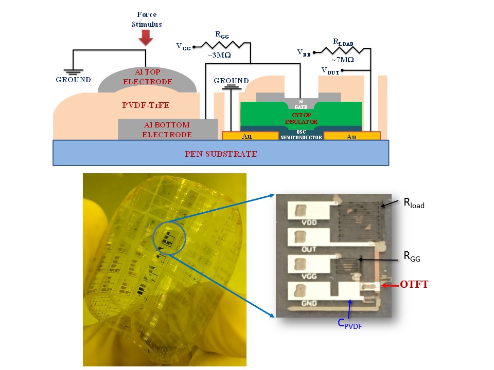
High performance solution processed OTFTs are exploited to fabricate flexible tactile sensors with POSTFT configuration. The sensor includes a thin piezoelectric capacitor, based on PVDF-TrFE sensing film, integrated with an OTFT and ink-jet printed resistors. The sensors show linear responses for stimulus with variable pressure and frequency.
Contact: Dr. Luigi Mariucci (luigi.mariucci@cnr.it)