
The research and study of microwave signals and technology have a huge impact in the society, as they form the basis for communication, remote sensing and modern navigation systems. In addition, the microwave sources are the main sources of energy in the food industry. Microwaves are used for the development and growth of materials in the semiconductor industry, and for the development of plasma technologies in medical equipment and surgical. In the design of these devices, engineers make use of the special properties of the propagation of microwave signals or their short wavelengths, large bandwidths and the existence of resonance frequencies related to molecular, atomic or nuclear properties. An aspect common to all existing applications is the property of microwaves to interact with objects of a size comparable with or greater than their wavelengths, i.e. from centimeters (cm) to millimeters (mm). With the advent of nanotechnology, the chance to explore the interaction of microwaves with much smaller objects (from micrometers to nanometers) is emerging as an exciting field of research and technological development.
The Scanning Microwave Microscopy (SMM) is proving to be of great interest for the analysis of surface and sub-surface samples and broad-spectrum devices, including both composite materials and devices for applications in microelectronics and sensors, even including biological tissues (e.g. cell membranes). The ability to determine the composition of biological materials at very small length scales is crucial for a wide range of applications, from nano-composites engineering and characterization to label-free detection for biomedical diagnostics and therapy.
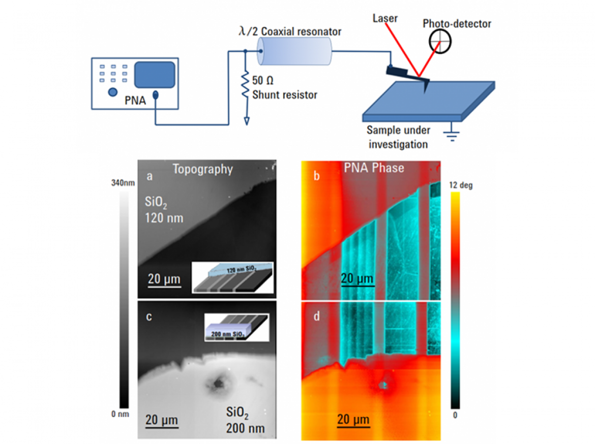
The Scanning-probe Microwave Microscopy is currently studied in our Unit with modelling efforts and homemade setups for the characterization at the micro-scale in a broad range of applications, ranging from materials to life sciences. New antennas, purposely designed sample-holders and micron-size probes are currently developed by means of chemical and physical etching techniques for broadband measurements. A multi-functional approach for the micro- and nano-antenna systems is followed, integrating the electrical matching as well as the probe and resonating elements to enhanced the measurement sensitivity. The characterization goals are, in particular:
- measurement of the sub-surface distribution of complex permittivity in thin and thick film dielectrics,
- sub-surface measurements of the structure and composition of nanocomposite materials, and nanostructured matrix materials,
- dielectric and magnetic permeability constants measurement,
- composition characterization of complex small scale nanostructures like core-shell nanoparticles,
- sub-surface monitoring of cellular processes in biology, including nanoparticle uptake for drug delivery.
TRL=4 can be obtained for the most part of the studied configurations.
POC: Romolo.Marcelli@artov.imm.cnr.it, Andrea.Lucibello@artov.imm.cnr.it, Emanuela.Proietti@artov.imm.cnr.it, Giovanni.Sardi@artov.imm.cnr.it, Giovanni.Capoccia@artov.imm.cnr.it, Bartolucci@eln.uniroma2.it