
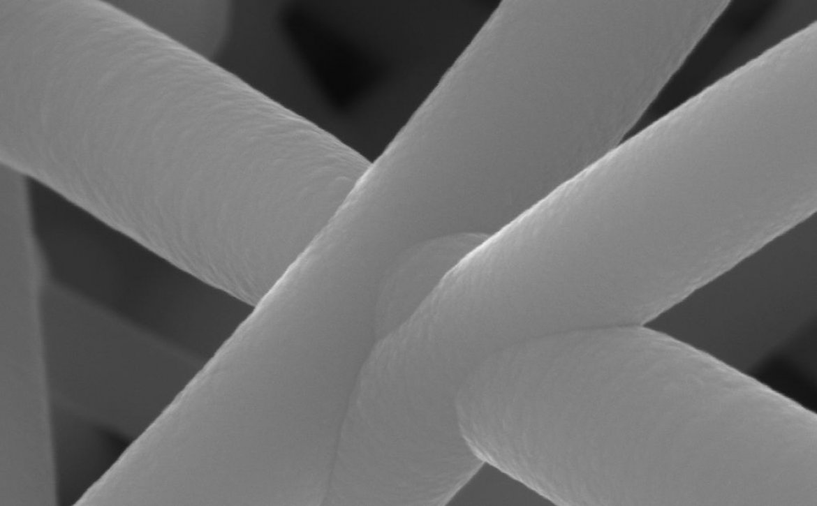
Semiconducting nanowires will become important building blocks of the next generation of miniaturized devices. Devices like sensors, light emitters, photovoltaic cells will take advantage of the small dimension of these nanostructures and of the unique features that nanowires offer with respect to their bulk counterpart as, e.g., a larger surface-to-volume ratio, the thermoelectric effect in silicon, the formation of wurtzite lattice structure in (N-free) III-V compounds, the stronger polarization dependence of light coupling as well as light wave-guiding.
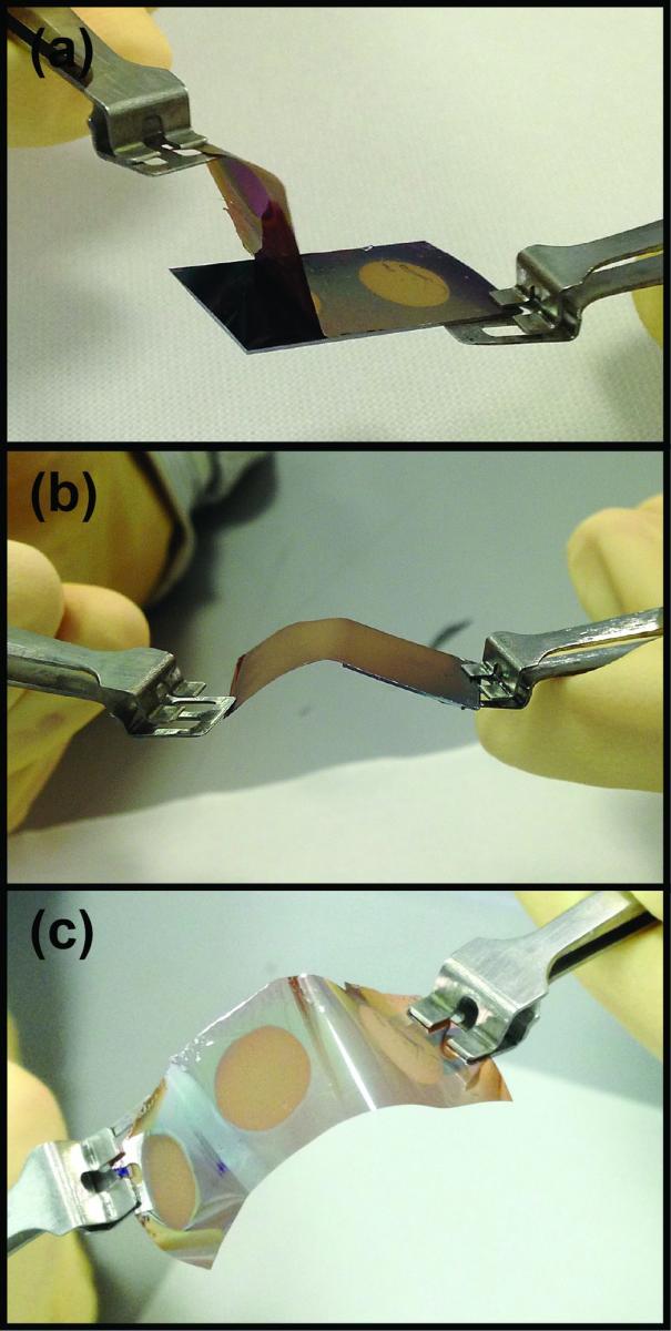
Arrays of semiconductor nanowires can be grown on any substrate that stands the growth conditions. This is due to the lack of lattice parameter constraints, which are instead typical of the epitaxial growth. Hence, low-cost, glassy and plastic substrates can be in principle used and are used to grow nanowires. Ordered or disordered arrays will be obtained depending on substrate, growth technique and/or growth conditions.
The activity on semiconductor nanowires at IMM-Rome started in the late 2008 as the natural continuation of the pioneering activity begun at TASC-INFM (now IOM-CNR) a few years earlier. The research on III-V and II-VI compounds (grown at IOM, in Trieste) has continued with particular focus on the optical properties and a new line was opened on silicon nanowires grown by plasma-enhanced chemical vapour deposition.
Research topics include (but are not limited to):
- the search for growth seeds alternative to gold (the most used metal to induce the growth but incompatible with the silicon technology platform)
- the growth without the use of any metal seed (self-catalysed growth)
- the determination of the band structure of wurtzite GaAs nanowires
- the optical properties of III-V, II-VI and Si nanowires
Beyond growth, the main experimental activities include continuous-wave and time-resolved photoluminescence, Raman, continuous-wave and fast-transient transmission. Synchrotron radiation is often used for particular studies. Fabrication facilities located in our clean room are used to obtain special nanostructures like hollow or telescopic nanowires.
The research is carried out in close cooperation with IOM-CNR in Trieste (https://www.iom.cnr.it/molecular-beam-epitaxy-mbe-laboratory) and with ISM-CNR in Rome (http://www.ism.cnr.it/en/efsl/)
Contact: Faustino Martelli (https://unit.artov.imm.cnr.it/users/fmartelli)
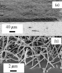 Si nanowires. The sample is inclined by 60◦. Notice the abruptness of the border between regions with and without wires because of different substrate parts treatment. (b) Detail of (a); the homogeneous morphology of the wires in all their length is apparent. Nanotechnology 21, 255601 (2010) |
 Nanotechnology 23, 305602 (2012) J. of Applied Physics 116, 174310 (2014) |
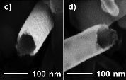
 In- [(a) and [(c)] and Au- (b) seeded silicon nanowires grown on polyimide Nanotechnology 27, 225601 (2016) |
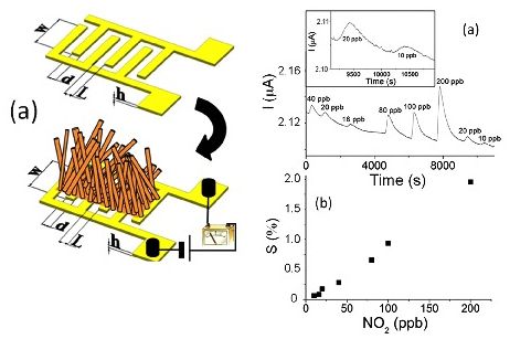 Left: (a) Sketch of the interdigitated structure used to realize the sensor and the designed Si NW sensor. In this case the disordered growth of the nanowires can be exploited to obtain self-welded nanowires that improve the device conductivity. Right: (a) Response curve of a typical sensor. The sensor response is the current change due to NO2 concentration variation at a bias voltage of 1 V. The inset shows the response and recovery behaviors of the device at 20 and 10 ppb. (b) Normalized current variation as a function of NO2 concentration at selected response time of 3 min. Appl. Phys. Lett. 101, 103101 (2012) |
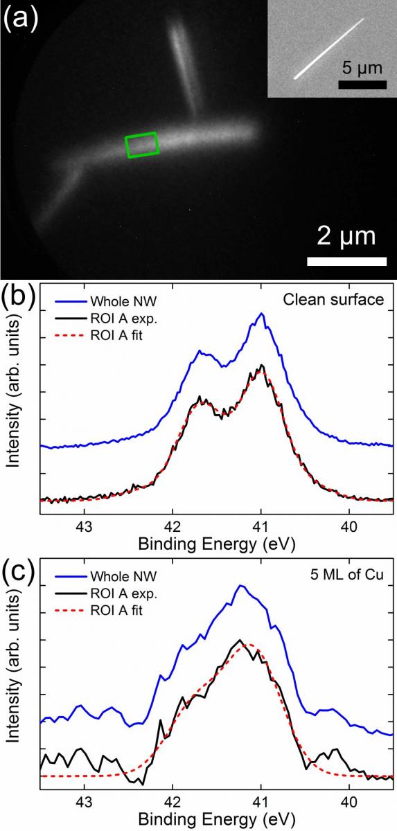 (a) XPEEM As3d imaging of a GaAs:Te nanowire with indicated the region, where the Schottky barrier was estimated. In the inset we report the image of a nanowire taken in a scanning electron microscope after the measurements. Notice that because of the very different technique of imaging and their visual quality, apparent size differences between the XPEEM and the SEM images could be observed. (b) XPEEM As3d spectra on the clean surface: the upper blue line is taken over the whole wire, while the lower black line is taken on the framed section of the wire (see (a)). The red curve is the cumulative fit to the spectrum in the framed region. (c) same as in (b) but for a Cu coverage of 5 ML. Applied Surface Science 386, 72 (2016) |
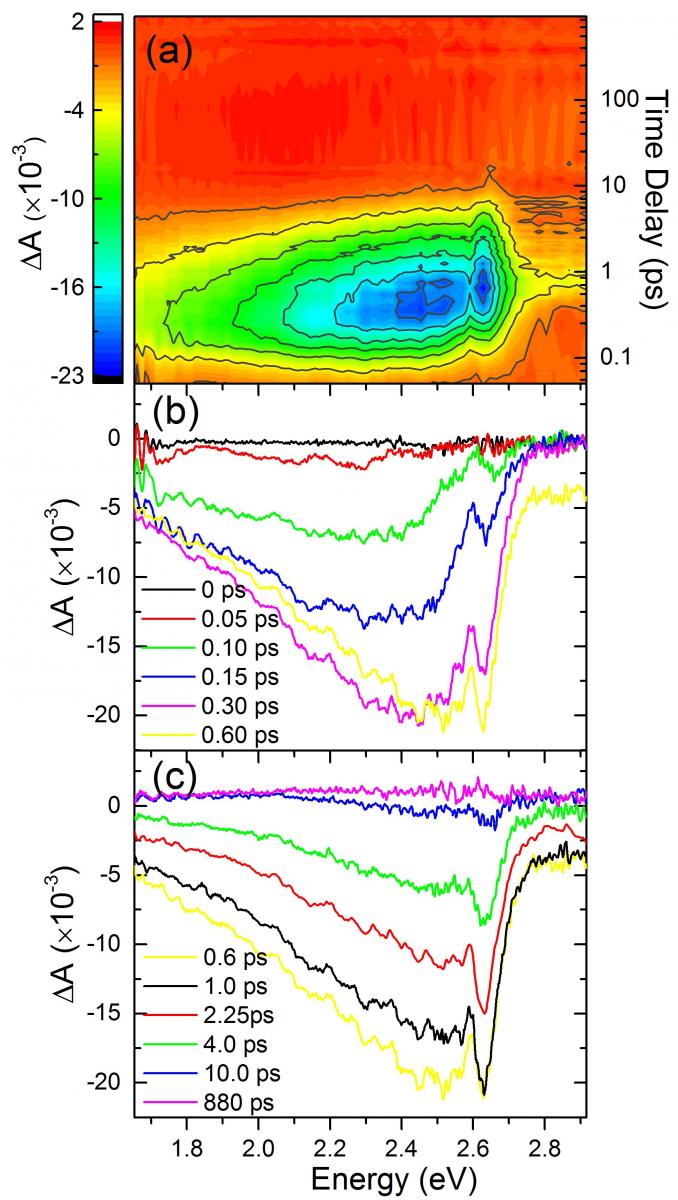 (a) Two-dimensional color map of the absorbance difference ΔA as a function of probe energy (x-axis) and of the delay time between pump and probe (y-axis). Notice the logarithmic scale of the y-axis. (b) Spectral dependence of ΔA for different delays, up to 0.6 ps. In this region the absolute value of ΔA increases for increasing delays. (c) Same as (b) but for delay times from 0.6 to 880 ps. In this time region the absolute value of ΔA decreases as the time delay increases. Physical Review B 94, 165442 (2016) |