
|
The activity of material synthesis at IMM Rome has two main objectives:
The main following activities are: |
|
| Plasma Enhanced Chemical Vapor Deposition (PECVD) | |
|
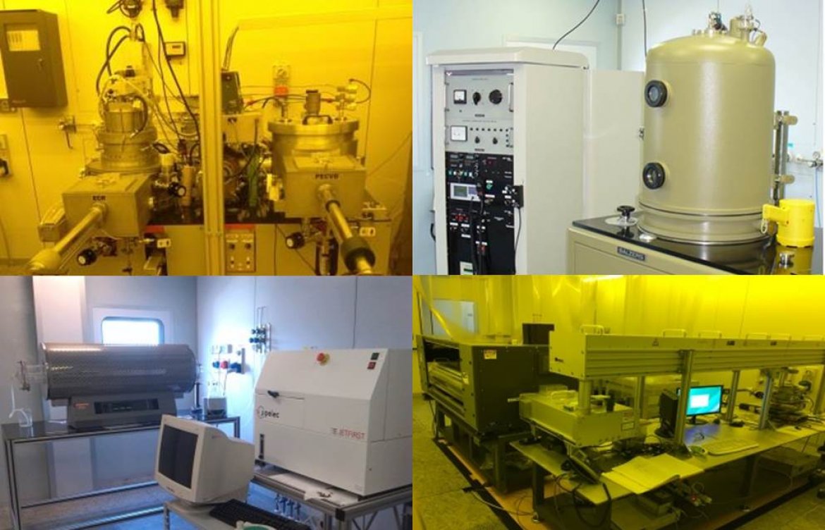
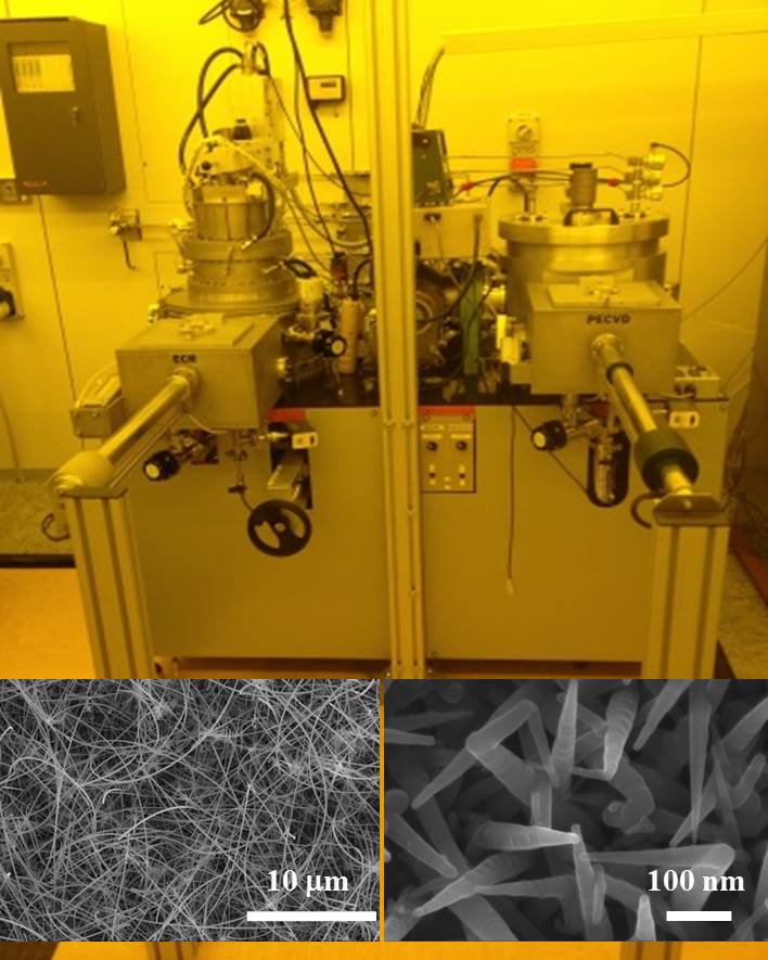
PECVD and Electron Cyclotron Resonance(ECR)-PECVD systems: SiH4, H2, N2O, NH3, PH3 B2H6, as process gases.
Scope: growth silicon (Si) based materials: Si nanowires (Si NWs), planar amorphous Si, planar silicon nitride (SiN) and silicon dioxide (SiO2). |
 |
| Thermal Evaporation | |
|
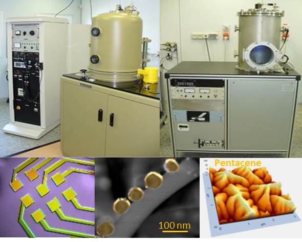
Balzers 510 evaporation system with electron beam and a thermal evaporation sources for the deposition of metals. Custom-made system for evaporation of organics.
Scope: evaporation of standard metal films for microelectronics (Au, Ag, Al, Cr, Ti, Pt, Ni, In etc.), Pentacene and nanowire decoration with metal nanoparticles (Au, and Ag). |
 |
| TF Sputtering | |
|
VS-40 Sistec sputtering sytem equipped with three catode (actually Titanium, Alluminum and Cromium target mounted) able to perform RF and DC sputtering deposition.
Scope: Deposition of thin films of ZnO, ITO and metals. |
 |
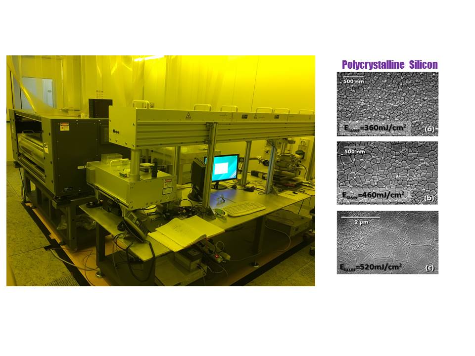
| Laser annealing | |
|
Excimer laser light at 308 nm and pulse duration approx. 30 ns.
Scope: Fabrication of polycrystalline Si, polycrystalline Si/Ge alloys, dopant activation by excimer laser irradiation. |
 |
| Contact person: Annalisa Convertino | |