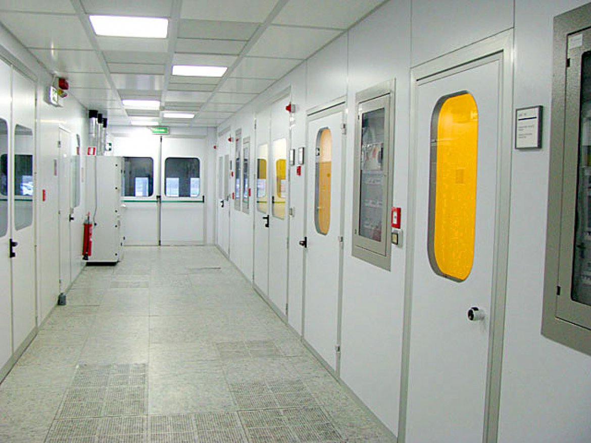
In the IMM-Rome a 300 sq. meters of class 1000-10000 controlled environment is available, located on the ground floor of the building, and used for research in solid state, optoelectronics, photonics, nanotechnology, micro-fabrication, MEMS, etc. This site is intended to be a resource for on-site IMM-Rome users as well as visitors doing research in micro-fabrication and semiconductor processing. It contains a large amount of reference material, relevant to micro-fabrication and semiconductor processing.
| Optical and laser lithography | |
|
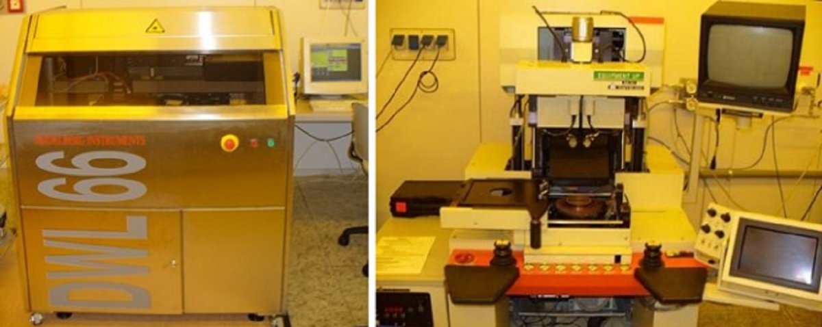
The laboratory is inside a clean room ISO 5-6 (class 100-1000). It comprises all the facilities to define micro patterns on planar substrates by means of contact optical lithography with a resolution down to 1 um.
|
|
| Wet and dry etching | |
|
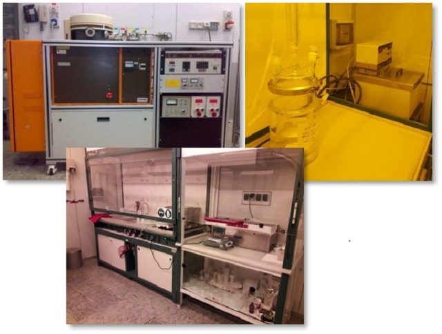
This laboratory is dedicated to isotropic and anisotropic etching of thin films a by wet and dry processes. Here are located also the facilities for substrate and photolithographic mask surface cleaning.
|
|
| Growth, deposition and thermal processes | |
|
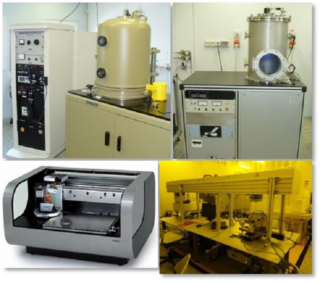
This laboratory is dedicated to isotropic and anisotropic etching of thin films a by wet and dry processes. Here are located also the facilities for substrate and photolithographic mask surface cleaning.
|
|
| Metrology, control and electrical characterization | |
|
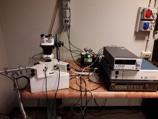
The laboratory is dedicated to perform the measurements necessary for on-line verification of process steps and to evaluate the electrical performances on test structures and devices at wafer level. Both manual and automatic systems are available.
|
|
| Simulation and design | |
|
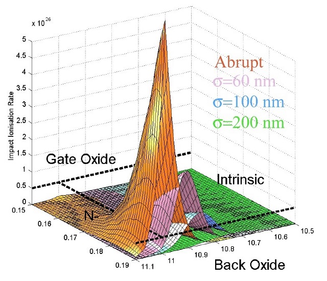
The micro- and nano-fabrication activity is supported by a corresponding activity on process numerical simulations. With process simulation it is possible to accurately predict the device geometry, its dopant distribution, and, with the help of device simulation software, also its electrical behavior. Several different scientific software are available in IMM-Roma and they are routinely used in the numerical simulation activity.
|
|


